 EMZETT.
Wafer
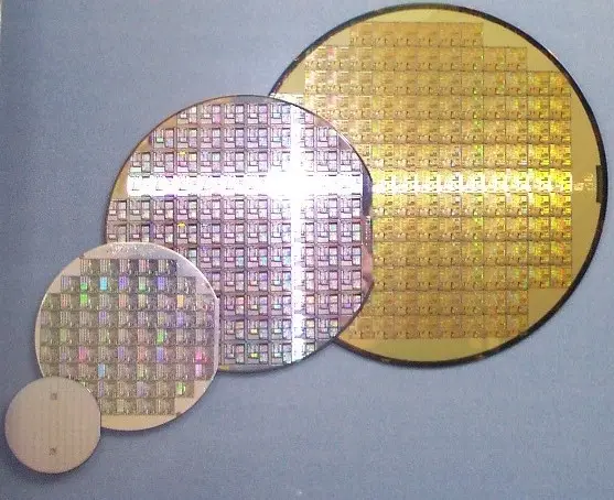 Image: German Wikipediabiatch, original upload 7. Okt 2004 by Stahlkocher de:Bild:Wa…, CC BY-SA 3.0, Wikimedia Commons


In short: A thin, round disc of high-purity silicon, on which many identical chips (“dies”) are exposed and etched at once during chip manufacturing.
In more detail: After manufacturing, the wafer is sawn into individual dies. The larger the wafer (today usually 300 mm in diameter) and the smaller the individual die, the more chips can be obtained from one wafer — a central cost factor in semiconductor production.
In Depth
Manufacturing a wafer begins with high-purity silicon, grown as a crystal, which is sawn into thin discs and polished. On this disc, the actual circuit structures of the individual dies are then built up layer by layer, in many consecutive steps (exposure with UV/X-ray light through extremely fine masks, chemical etching, doping with other elements to specifically alter electrical properties) — a modern chip can consist of several dozen stacked structural layers.
Not every die on a wafer ends up working correctly — manufacturing defects usually occur randomly distributed across the wafer surface (“yield”, the proportion of usable dies per wafer). Larger dies statistically have a higher probability of being hit by a defect than smaller ones — one reason very large, complex chips (e.g. high-end graphics processors) are disproportionately more expensive relative to their chip area than smaller chips. Chip manufacturers sometimes sort functional but slightly defective dies into cheaper product variants with a reduced core count or lower clock speed, instead of discarding them (“binning”).
Wafer foundries as their own business model
Not every company that designs chips also manufactures them — specialised “foundries” (contract manufacturers) own the extremely expensive manufacturing facilities and produce wafers on behalf of various chip design companies that don’t have their own factory (“fabless”). A modern chip factory now costs several billion euros/dollars in investment, which is why this contract model is economically more worthwhile for most chip designers than running their own manufacturing and keeping it permanently at the latest technological level.
Exposure steps and manufacturing time
Producing a finished wafer goes through hundreds of individual manufacturing steps over several weeks — each of the many stacked chip layers needs its own, highly precise exposure with special masks, followed by etching, cleaning and testing, before the next layer can be applied. A single manufacturing defect early in the process can affect all subsequent layers, which is why the manufacturing environment (clean rooms with extremely low particle contamination) is among the most demanding industrial environments there are.
See also: Die (Semiconductor), Silicon Chip